· Editor · 12 min read
Multi Chip Module (MCM) Technology: Types, Benefits, and Applications
A multi chip module mounts several integrated circuits on one high-density substrate inside a single package, cutting interconnect distance for faster signals and lower power.
Key Takeaways
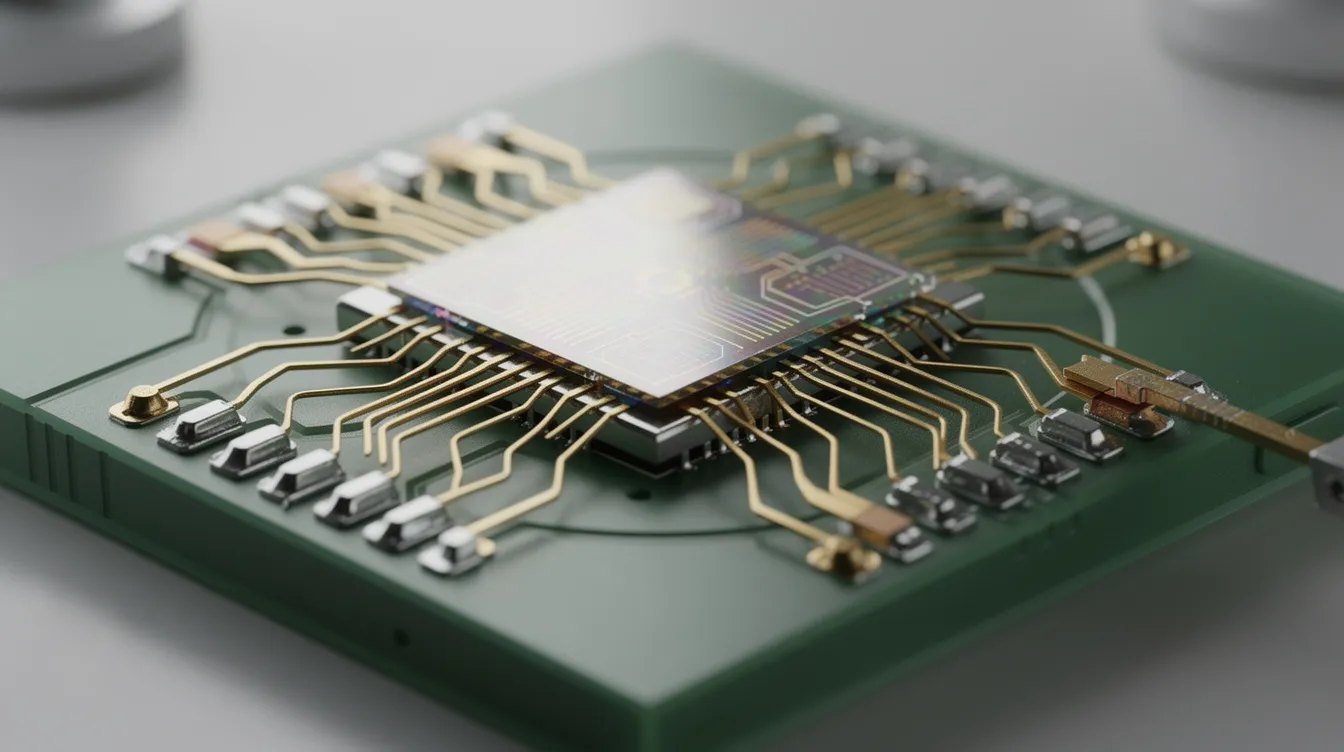
A multi chip module MCM mounts multiple integrated circuits on one high-density substrate inside a single package. This replaces several discrete components on a printed circuit board.
MCM technology cuts interconnect distance between dies. That means faster signal propagation, lower power consumption, and improved electrical performance.
Engineers classify multi chip modules by substrate: MCM-L (laminate), MCM-C (ceramic), MCM-D (thin film), MCM-D/C (hybrid), and MCM-Si (silicon interposer). Each type fits different cost and performance targets.
Designing an advanced MCM package involves thermal management, signal integrity, manufacturing tolerances, and Known Good Die testing.
MCM technology powers products in data centers, 5G infrastructure, automotive electronics, aerospace, and artificial intelligence accelerators.
Introduction to Multi Chip Modules (MCMs)
MCM technology emerged in the 1980s to meet complex system requirements in supercomputers and defense electronics. Traditional chips are single-chip designs. MCMs take a different path: they mount two or more bare dies on one substrate to act as a single unit.
The semiconductor industry now faces growing demand from artificial intelligence, 5G, and autonomous vehicles. These workloads need more transistors, more memory bandwidth, and lower latency. MCMs answer that call. They enhance performance by integrating multiple chips into one module. Marvell’s 2025 packaging platform, for example, enables modules 2.8× larger than single-die accelerators while cutting total cost of ownership.
This article covers MCM key characteristics, types, assembly processes, applications, and how the multi chip module compares with SoC and system in package solutions.
What Is a Multi Chip Module?
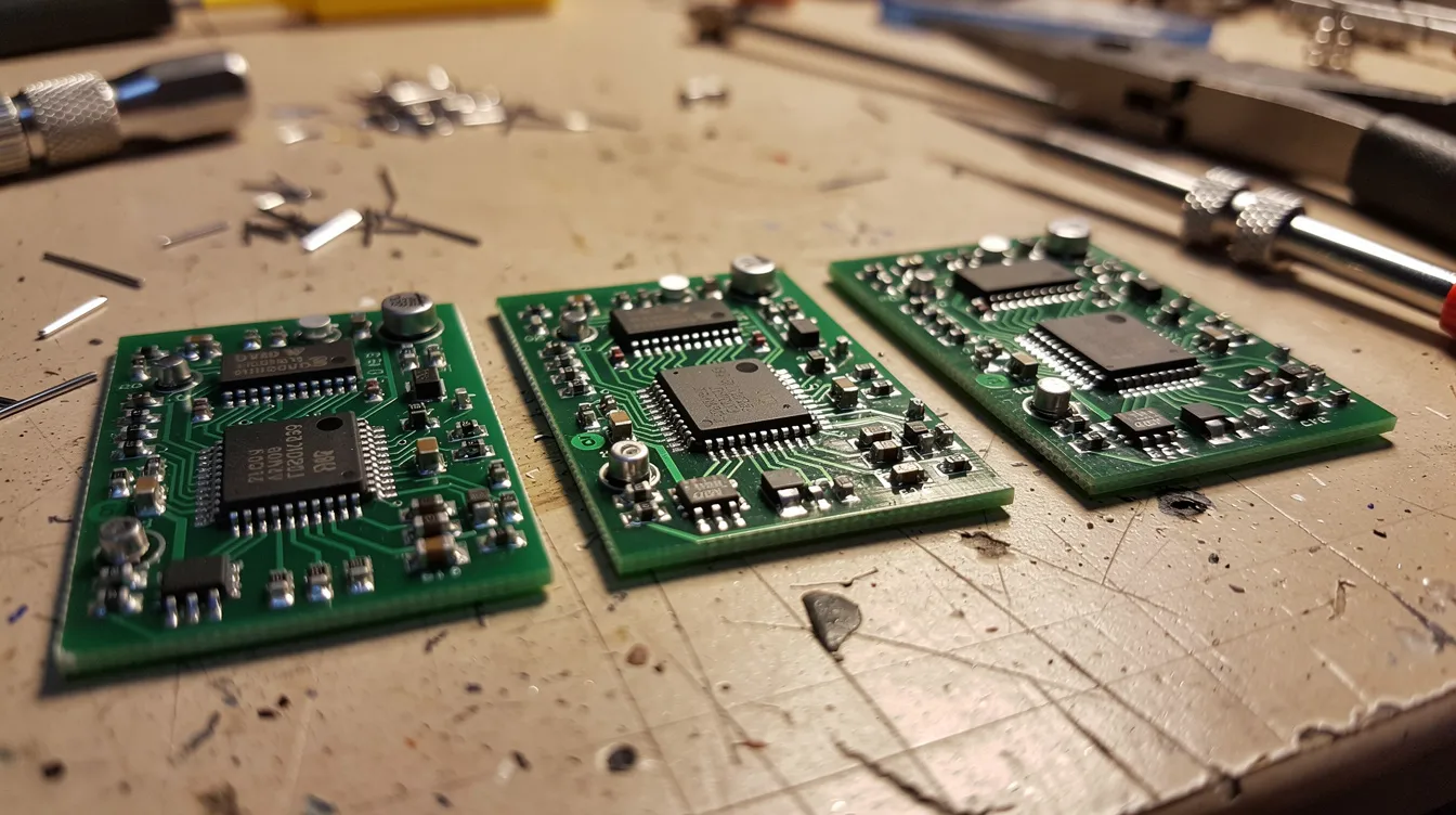
A multi chip module MCM is an electronic assembly that integrates multiple integrated circuits and passive electronic components on one high-density substrate inside a single package. MCMs integrate multiple chips into a single package. The result looks and acts like one cohesive unit to the rest of the system.
An MCM replaces several individual packages on a board. It reduces interconnect distance for faster signal propagation. Typical substrate materials include ceramic substrate options, organic substrates (laminates), and silicon interposer platforms. Common interconnect methods are wire bonding, flip chip with solder bumps, and microbumps for fine-pitch connections.
Where does a multichip module sit in the system hierarchy? Between the bare die level and the printed circuit board. It bridges the gap, offering much denser routing than a PCB but without forcing all functions onto one monolithic die.
Key Characteristics of Multi Chip Modules
The key characteristics of MCM technology fall into three groups: structural traits, performance traits, and reliability traits.
Structural traits include:
Multiple dies on one substrate with high density interconnections
Controlled impedance lines and compact form factor
Multilayer ceramic substrate or organic routing with fine vias
Thin film interconnect layers for dense signal paths
Performance traits include:
Higher bandwidth between dies due to shorter paths
Lower signal delay and reduced parasitics
Improved electrical performance at multi-gigabit speeds
Electrical performance is a primary consideration in MCM design. It minimizes signal interference between neighboring channels. Interconnect density affects signal integrity, so designers balance routing density against crosstalk. Power distribution networks in MCMs must minimize voltage drops and noise across the substrate.
Substrate material influences the electrical and thermal performance of the entire module. A ceramic substrate offers low loss at high frequencies. An organic substrate costs less but has higher dielectric loss.
For reliability, MCMs offer improved reliability through careful die screening, thermal paths through substrate and lid, and maintaining signal integrity across temperature cycles.
Why Use Multi Chip Modules Instead of Single-Chip Packages?
Every designer faces a choice: keep everything on a single monolithic chip, or split functions across a multi chip module architecture. Each path has trade-offs.
MCMs bypass the physical limitations of massive monolithic system-on-chips. A large SoC die suffers steep yield losses as area grows. MCMs reduce overall system size and weight compared to multiple standard packages on a board. That matters in aerospace and space constrained applications.
MCMs minimize interconnect distance, enabling faster signal propagation between dies. A 2025 IEEE study on memory-centric MCM-GPU architecture measured 1.36× average performance gain, up to 1.90×, over GPU-centric designs. MCMs can provide better performance than monolithic ICs under specific integration scenarios like these.
Different semiconductor technologies can be integrated using MCMs. A designer can place a 5 nm CPU die next to a 28 nm analog block and a 65 nm RF front-end. Coordinated chip integration across different process technologies is a core strength. This heterogeneous integration is impossible on a single monolithic die.
Monolithic chips still dominate cost sensitive applications with high volumes. MCMs cost more per unit due to complex assembly, tighter manufacturing tolerances, and extra test steps.
Types of Multi Chip Modules (MCM-L, MCM-C, MCM-D, MCM-D/C, MCM-Si)
Engineers classify MCMs by substrate material and manufacturing method. Common types of MCMs include MCM-L, MCM-C, and MCM-D. Each serves different cost and performance goals.
MCM-L (Laminate): Uses organic substrates similar to standard PCBs, but with finer lines and smaller vias. MCM-L offers a balance of cost and manufacturability. Best for commercial electronics, networking gear, and cost sensitive applications.
MCM-C (Ceramic): MCM-C uses ceramic substrates for enhanced durability. The multilayer ceramic substrate handles high temperatures and provides hermetic sealing. Designers choose this for automotive electronics, aerospace, and defense where thermal behavior and ruggedness matter.
MCM-D (Thin Film): MCM-D employs thin-film technology for high-performance applications. Conductors and dielectrics are deposited via sputtering and photolithography. Line widths drop below 25 µm. Cost and design complexity are highest in this category.
MCM-D/C (Hybrid): Combines a ceramic body with thin-film deposited layers for signal routing. Suited to rugged, high performance systems that need both routing density and mechanical robustness.
MCM-Si (Silicon Interposer): MCM-Si utilizes silicon substrates for specialized high-end systems. A silicon interposer supports through silicon vias and microbumps at pitches as tight as 25 µm. This type underpins modern GPU, FPGA, and AI accelerator packages using TSMC’s CoWoS-L platform.
3D and High-Density Multi-Chip Modules
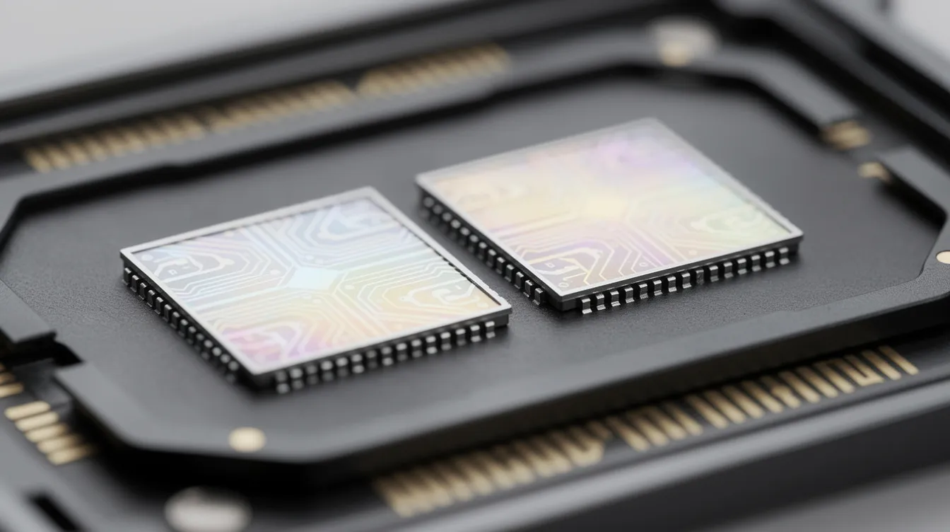
3D multi-chip modules stack multiple dies vertically. Connections run through through silicon vias, hybrid bonding, or microbumps. Vertical stacking cuts footprint and boosts bandwidth.
High Bandwidth Memory integration is critical for AI applications using MCMs. HBM stacks sit directly over logic dies. This layout shortens the path between processor and memory to fractions of a millimeter. The result: massive bandwidth gains and improved power efficiency.
Short vertical interconnects deliver lower signal delay and better power efficiency than side-by-side layouts. These modules serve high performance computing and data centers running large language models and training workloads.
Challenges remain. Heat dissipation from inner dies is hard to manage. Mechanical stress builds between layers with different thermal requirements. The assembly process grows more complex, and test flows must verify each die and its vertical connections.
2.5D solutions with a silicon interposer act as a bridge. They keep dies side by side on an interposer instead of stacking them. This avoids the worst thermal problems while still shortening interconnect distance.
MCM vs System-in-Package (SiP) and SoC Integration
Engineers pick from three main integration paths: multi chip module, system in package, and system-on-chip. Each fits different markets.
An MCM is a subsystem or chip module focused on tightly coupled multiple functions. It prioritizes high speed interconnects and performance density between a few dies. SiP technologies target a whole system: processor, memory, RF, passives, and sensors in one package. SiP suits mass-market consumer devices like smartphones and wearables.
SoC integration puts multiple functions on one monolithic die. That helps cost in high-volume runs. But it locks all blocks into one process node and risks large-die yield losses. MCMs and SiPs support heterogeneous integration across different process nodes, using the best manufacturing process for each function.
SoCs demand high non-recurring engineering investment. MCM and SiP solutions can re-use chiplets and redistribution layer designs. That shortens design schedules and cuts system design cost for low-to-medium volume products.
Assembly Processes and Interconnect Technologies in MCMs
The assembly process and interconnect choices determine MCM performance and improved reliability. Small errors in placement or bonding can ruin an entire module.
Common die attach and interconnect methods:
Wire bonding for lower-cost connections
Flip-chip with solder bumps for dense I/O
Microbumps for fine-pitch below 50 µm
Hybrid bonding for direct copper-to-copper contact
Substrate build-up involves multilayer conductors, laser-drilled vias, and controlled impedance traces. IBM’s MFIT platform achieves die placement accuracy of ±40 µm at 45 µm pitch and ±15 µm at 25 µm pitch. It supports UCIe Advanced at 32 Gbps and HBM3e at 9.6 Gbps.
Known Good Die testing is essential for MCMs to prevent defects in multi-die packages. One bad die wastes the entire module. Ultra-thin substrates are delicate and complicate manufacturing processes. Manufacturing yield optimization is complex in MCM technology, so assembly services invest in precise reflow control, underfill application, and thermal interface materials.
Applications of Multi Chip Modules Across Industries
MCM technology already ships in volume products across several industries.
High performance computing and data centers: GPU modules pair logic chiplets with HBM stacks on silicon interposers. MCMs support high-bandwidth memory applications in compact designs. Network switches and AI accelerator cards rely on multi chip modules for the bandwidth that artificial intelligence workloads demand.
Telecommunications and 5G: MCMs are suitable for high-frequency RF front-ends and baseband processors. MCMs support high-speed data transfer in telecommunications for 5G networks. Massive MIMO radios and baseband units need compact, high-bandwidth chip modules. The JEDEC SPHBM4 standard may reduce interposer costs in these applications.
Automotive and industrial: Automotive systems use MCMs for Advanced Driver-Assistance Systems integration. MCMs are essential in autonomous vehicles for compact electronics. MCMs enable integration of chips for sensor technologies in vehicles, including radar and lidar modules.
Aerospace and defense: MCMs are used in aerospace applications for miniaturization and weight reduction. Ceramic packages provide hermetic sealing for long-life missions.
Consumer and edge devices: MCMs improve performance in consumer electronics like smartphones and tablets. Gaming consoles, VR headsets, and IoT gateways use multi chip integration to balance power efficiency, size, and cost.

Benefits and Trade-Offs: Performance, Power Efficiency, and Cost
MCM design is always a trade-off among device performance, power efficiency, and manufacturing cost.
Performance gains: MCMs improve device performance by integrating multiple functions into one module. Bandwidth per millimeter between dies is far higher than between discrete components on a PCB. Lower signal delay and better signal integrity appear at multi-gigabit speeds.
Power efficiency gains: MCMs reduce power consumption by shortening interconnects and simplifying assembly processes. Shorter paths cut dynamic switching power. Optimized power delivery networks on the substrate reduce distribution losses. One 2025 study reported up to 2.7× energy-delay product improvement through hardware-software co-optimization of MCM interconnects.
Cost factors: Advanced packaging technologies add substrate complexity, complex assembly steps, and more test points. But using smaller dies improves yield per die. Mixing different process technologies lowers per-function cost. MCMs enhance reliability by simplifying system assembly at the board level, reducing the number of various components a system integrator must handle.
When MCMs are justified: High performance systems, mission-critical electronics, and designs that need heterogeneous integration more than minimal unit cost.
Challenges and Future Directions in MCM Technology
Several technical and supply chain hurdles still limit wider MCM adoption.
Design challenges: Designing MCMs involves multidisciplinary considerations including thermal, mechanical, and economic factors. Co-design of dies and package is required. Power delivery integrity, clock distribution, and electromagnetic interference inside dense multichip modules all demand careful system design. Design verification is more challenging in multi-chip modules than in single-die packages. Manufacturing complexity rises with die count.
Thermal challenges: Thermal management is crucial for MCMs due to the proximity of multiple high-performance dies. Thermal management is critical because multiple active dies generate heat in a small area. MCMs generate concentrated heat loads which can lead to thermal throttling if not managed. MCM design must consider thermal coupling between neighboring chips to manage heat dissipation. Integrating heat spreaders, micro-channel coolers, or liquid cooling adds cost and package design complexity.
Manufacturing and test: The delicate nature of ultra-thin substrates complicates handling. Yield challenges grow as die count rises. Repair mechanisms at the die level do not exist; failed modules must be replaced as a single unit.
Future trends: Standardized chiplets and interface standards like UCIe will expand the chiplet ecosystem. TrendForce forecasts that CoWoS-L reticle usage will scale from ~3.5× to ~9× by 2027. EMIB-T and fan-out interposers will compete for large-package designs. Broader adoption of 3D multi-chip modules in AI and edge systems is expected through 2030.
FAQ
These questions address practical concerns engineers and buyers often raise about multi chip modules.
How does a multi chip module differ from a standard PCB with several packages?
An MCM mounts bare dies on a high-density substrate. A PCB carries fully packaged ICs. The MCM substrate has finer routing, more layers, and controlled impedance lines. That produces shorter, cleaner high speed interconnects with lower parasitic capacitance. A standard PCB has longer traces, higher inductance, and worse signal integrity between chips.
Can I mix different process nodes and technologies in one multichip module?
Yes. A common example: combining a 5 nm digital die with a 65 nm RF die and discrete power devices on one multi chip module. This heterogeneous integration across different process nodes is a primary reason designers pick MCM technology over a single monolithic chip.
What design tools do I need for MCM layout and signal integrity?
Engineers use package-aware EDA tools that handle substrate stack-ups, 2.5D/3D structures, and electromagnetic field solvers. Co-simulation of die, package, and board predicts power integrity and signal behavior before fabrication. The design process must verify thermal, electrical, and mechanical behavior together.
How do multi chip modules affect product repair and field service?
MCMs act as a single sealed unit. Failed modules are replaced whole. Die-level repair is not practical. This means robust burn-in and screening matter. Organizations must plan maintenance strategy around module-level replacement, not component-level repair mechanisms.
When is a System-in-Package (SiP) a better fit than an MCM?
Designers choose SiP when they want a complete system (processor, memory, RF, passives) in one package for mass-market products like phones or wearables. MCM fits high performance subsystems and specialized chip modules where performance density and flexibility outweigh the need for extreme integration or minimal per-unit cost.