· Editor · 13 min read
Best Printed Circuit Board Assembly Options for Reliable Electronics Production
A printed circuit board (PCB) is a blank circuit board without components. It holds copper traces, a solder mask, and conductive pathways. But it cannot do anything on its own. PCBs are not
Introduction: What Printed Circuit Board Assembly Means for Your Products
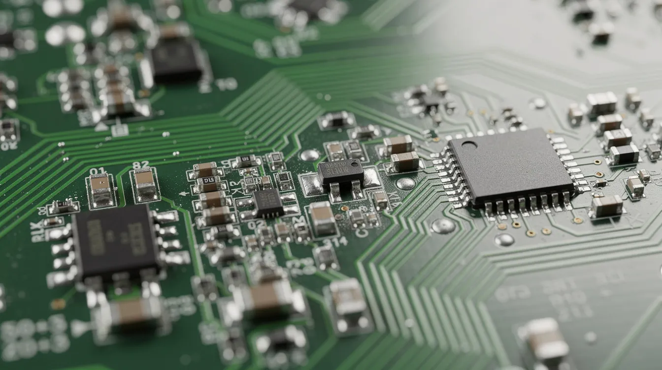
A printed circuit board (PCB) is a blank circuit board without components. It holds copper traces, a solder mask, and conductive pathways. But it cannot do anything on its own. PCBs are not functional until components are added through printed circuit board assembly.
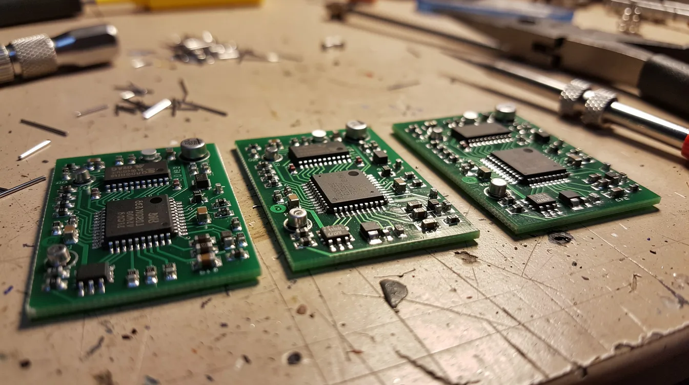
A PCBA includes a PCB with all electronic components installed. It is a completed assembly ready for electronic devices. Manufacturing a PCB is simpler than producing a PCBA. The assembly process adds integrated circuits, resistors, capacitors, and connectors to the bare board.
This article compares five distinct ways to get circuit board assembly (PCBA) done. You will see how in-house lines, domestic partners, overseas factories, prototyping services, and hybrid models stack up. The goal is to help you choose based on quality, lead time, cost, capability range, support, and risk. Ordering small-batch PCBA depends on priorities like cost and speed. The best PCBA company depends on your project stage. PCBA providers are segmented by strengths in prototyping, scalability, and reliability. Each section below gives concrete guidance and specific use cases.
How We Evaluated the Best Printed Circuit Board Assembly Approaches
We compared major PCBA sourcing models rather than specific brand names. The criteria reflect real project needs in 2024–2025 electronics manufacturing.
Quality and Reliability
PCB assembly services meet high standards when they follow IPC-A-610 and IPC-J-STD-001. These standards define visual acceptability and soldering requirements. ISO and IATF certifications are important for industry compliance. They form the baseline for quality assurance in any quality control system.
Design for Manufacturability checks are critical for high-reliability PCBs. DFM checks reduce manufacturing costs by identifying design flaws early. A common PCB design flaw - like incorrect pad dimensions or tight trace clearance - can cause costly re-spins.
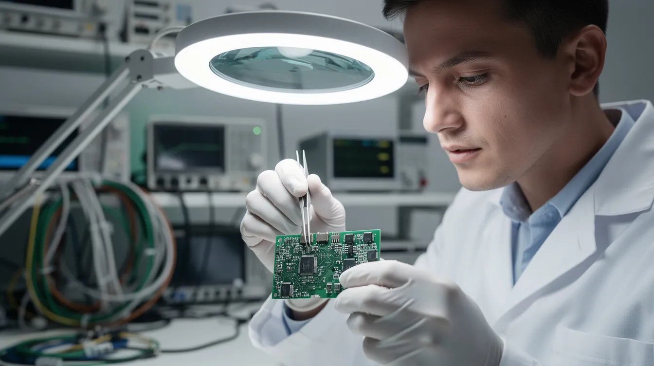
We also weighed testing methods. In-circuit testing is the most efficient method for PCB quality assurance. Automated optical inspection (AOI) speeds up quality checks for PCBAs. Automatic optical inspection uses high-powered cameras for PCB checks. It catches misplaced components and solder defects fast. X-ray inspections reveal hidden defects in complex PCBAs, like voids under BGA solder joints. Final functional tests ensure PCBAs meet performance standards before shipping. Final inspection tests PCB functionality under simulated conditions. Boundary scan testing adds another layer of verification for dense digital boards. A flying probe tester offers flexible coverage without custom fixtures. Flying probe testing works well for low-volume and prototype runs.
Capability and Technology Fit
We looked at whether each model can handle fine-pitch BGAs, 01005 passives, and high-layer-count boards. Support for rigid PCB and flexible PCBs matters. Flexible PCBs use high-temperature plastic like Kapton. Metal core PCBs dissipate heat more efficiently than FR4.
PCBs are made from fiberglass or composite epoxy. FR-4 is the most common PCB substrate material. Copper is the primary conductive material in PCBs. During PCB manufacturing, copper foil bonds to the substrate material through a lamination process. Unwanted copper is etched away to form the outer layers and conductive pathways. The PCB surface receives a solder mask to protect copper traces from an oxide layer and accidental shorts.
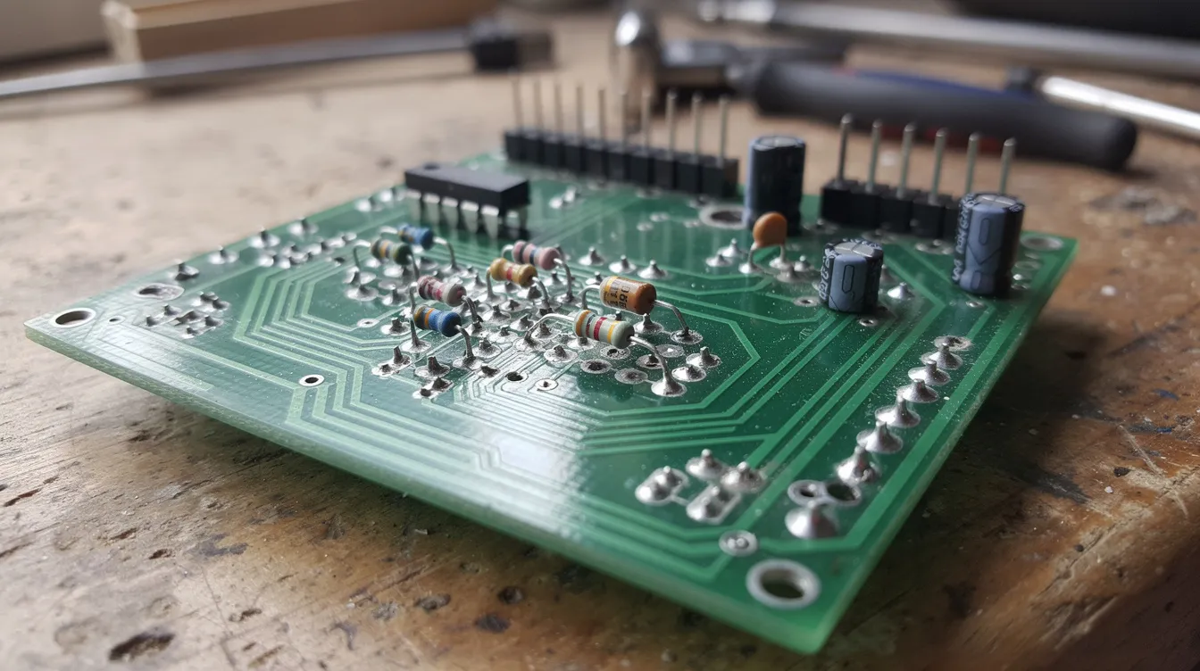
Surface mount technology allows placement of components on PCB surfaces. SMT allows for higher connection densities on the PCB board. Thru-hole technology involves inserting leads through PCB holes. The hole walls receive plating to ensure solid connections. A capable partner handles both SMT assembly and through-hole components. SMD assembly and thru hole components often appear on the same board. Special processes like conformal coating, selective solder, and burn-in testing also shaped our evaluation.
Lead Time, Capacity, and Scalability
Prototype lead times range from 5 to 15 calendar days. High-volume builds take 3 to 6 weeks. PCB assembly capacity varies by manufacturer from prototypes to mass production. Turnaround time is crucial for prototyping projects.
The ability to scale from 10 prototypes to tens of thousands matters. Capacity buffers during ramps and seasonal demand spikes also influenced our evaluation.
Cost, Transparency, and Total Value
We considered more than unit price. NRE charges, stencil costs, test fixture costs, and shipping all factor in. A transparent quote with a full BOM breakdown and clear labor assumptions ranks higher.
For a simple board with about 50 SMT components at 100 units, assembly in China runs about $5–$15 per board. The same board in the U.S. costs $25–$50. But tariffs, freight, and rework close this gap. After adding duties and shipping, the cost advantage often drops from 2.5–3× to about 1.3–1.6×. Manufacturing costs include BOM (about 61%), PCB fabrication (about 23%), assembly labor (about 13%), and tooling (about 3%).
Supply Chain and Component Management
Turnkey providers manage component sourcing and assembly. This model simplifies logistics. But it adds markup and risk of long-lead parts. Consignment gives you control. It also increases your procurement burden.
Strong vendor relationships with distributors like DigiKey, Mouser, Arrow, and Avnet influence lead time and risk. Obsolescence management and substitution control also shaped our evaluation.
Communication, Location, and Support
Time zone alignment, language, and engineering support during DFM reviews matter. Fast response to design issues and ECOs can save weeks. U.S.-based manufacturers offer advantages in regulatory compliance. On-site visits and audits are easier with a domestic partner. These factors weigh heavily for long-term manufacturing partnerships.
Best 5 Printed Circuit Board Assembly Options for Different Needs
Below you will find five distinct ways to get PCB assemblies built. Each option is ranked by fit for common use cases. These are models - not specific brands - so you can match each one to your situation.
1. Domestic Turnkey Contract Manufacturer
A domestic turnkey contract manufacturer is a full-service EMS partner based in the same country as you. Think U.S., U.K., or Germany. This partner handles everything from PCB fabrication sourcing to SMT and THT assembly. They also run testing, box build, and logistics.
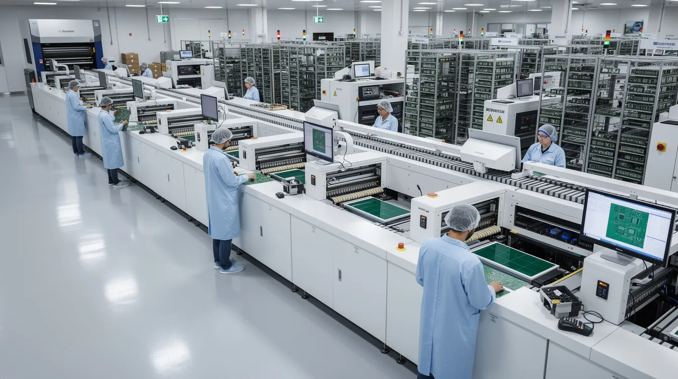
The PCBA assembly process at a domestic EMS follows proven steps. A solder paste printer applies solder paste onto the board. Lead free solder paste consists of 96.5% tin, 3% silver, and 0.5% copper. The printer deposits a thin layer of paste onto each pad. A pick and place machine then handles component placement. It positions all the components - from small components like 01005 passives to large connectors. Reflow soldering heats PCBs to around 250 degrees Celsius inside a reflow oven. The reflow process melts the paste and forms solid solder joints. For through-hole parts, wave soldering washes molten solder over PCB leads for connections. The solder wave flows across component leads in a controlled pass. Wave soldering automates the soldering of thru-hole components.
Why It Stands Out
Domestic turnkey EMS excels at communication. Audits are simple. Issue resolution happens fast. IP protection is stronger. High-reliability manufacturers support complex industries like aerospace and defense. PCB assembly services meet stringent regulatory needs here.
Best For
Startups with complex hardware and certification needs
Mid-size OEMs seeking a long-term assembly partner
Companies needing UL, FDA, or CE compliance support
Key Strengths
Engineering DFM support before production starts
Full traceability from component lot to final board
Mature quality systems with IPC Class 2 or Class 3 compliance
Short domestic shipping times
Responsive ECO handling
Possible Limitations
Higher labor cost per board compared to offshore quotes
Minimum order sizes may be 25–50 units
Less cost advantage at very high volumes
Unit pricing looks high but can reduce total lifecycle cost
2. Overseas High-Volume PCBA Manufacturer
An overseas high-volume factory sits in regions like China, Vietnam, or Mexico. It focuses on cost-efficient production. Global EMS providers are best for large-scale production. They serve consumer electronics, IoT devices, and appliances. These factories build tens of thousands of boards per year.
Why It Stands Out
The main benefit is low per-unit cost for stable, repeatable builds at scale. Automated soldering techniques improve assembly precision. Advanced automation and panel optimization drive prices down.
Best For
Mature designs with frozen BOMs
High-volume deployments above 10,000 units per year
Cost-sensitive products with predictable demand
Key Strengths
24/7 production capacity
Aggressive per-placement pricing ($0.007–$0.02 per SMT placement)
Broad component sourcing networks
Advanced automated process lines with SMT components at high speed
Possible Limitations
Longer supply chains add weeks to delivery
Tariffs (e.g., 25% Section 301 duties on Chinese PCBA) raise landed cost
Language and time-zone friction slows communication
Rapid engineering changes are hard once mass production starts
3. Rapid Prototype PCBA Service
Rapid prototype services focus on quick-turn assembly. They handle 1 to 50 boards for engineering samples and early prototypes. Most offer online quoting and instant DFM feedback. You upload Gerber files, a centroid file, and your BOM. They handle the rest.
Why It Stands Out
Speed is the focus. Some services offer 24-hour to 5-day assembly for small runs. They apply solder paste, attach components, and run solder paste printing with standard stencils. Rapid prototyping is ideal for hobbyists and makers too.
Best For
Hardware startups iterating designs fast
R&D teams running EVT or DVT builds
University labs and proof-of-concept builds
Key Strengths
Low minimum quantities (even single boards)
Fast quoting - often within hours
Standard process flows that cover most designs
Some services stock common passives to reduce lead time
Optional rework services
Possible Limitations
Less focus on long-term cost optimization
Limited test coverage (may skip ICT or environmental tests)
Fewer special processes like conformal coating or potting
Higher per-unit cost due to fixed setup charges
4. In-House Printed Circuit Board Assembly Line
Some OEMs invest in their own SMT line, wave soldering process equipment, and test stations. This is common in high-mix, medium-volume industrial, aerospace, or defense companies. They own the entire manufacturing process.
Why It Stands Out
Full process control is the unique benefit. Feedback between design and manufacturing happens instantly. Sensitive IP stays internal. Adhering components to your own boards gives you direct oversight of every step. Manual soldering for rework or odd-form parts happens on-site. Automated processes reduce human error in PCB assembly. Automation in PCBA increases production speed on your own floor.
Best For
Companies with stable demand and many product variations
Firms with strict security or export controls (ITAR, EAR)
Long-lifecycle industrial systems with 10+ year support needs
Key Strengths
High flexibility for small batches and quick changeovers
Direct control over work instructions and process parameters
Deep process know-how stays in-house
Soldering electronic components under your own quality control rules
Possible Limitations
High capital expense for pick-and-place, reflow ovens, AOI, and X-ray equipment
Need for skilled operators and process engineers
Risk of underutilized equipment during demand dips
Ongoing maintenance and calibration costs
5. Hybrid Model: Local NPI + Offshore Volume PCBA
The hybrid model blends two partners. You build prototypes and first small batches with a local partner. Then you transfer the stable design to an overseas volume factory. Documentation and test fixtures bridge the gap.
Why It Stands Out
You get fast, high-touch support during the design phase. You get lower cost at volume later. Risk stays controlled during early debugging and certification. The PCB assembly process gets validated locally before handoff.
Best For
Growing hardware firms planning to scale from pilot to mass production within 12–24 months
Consumer and industrial IoT products with complex firmware
Products with frequent early revisions that stabilize before volume ramp
Key Strengths
Smoother design transfer with validated test plans
Reduced time to scale from NPI to production
Balanced cost and engineering support
PCB’s electrical characteristics get verified at each stage
Possible Limitations
Requires careful handover and dual qualification of processes
Strong documentation is essential
Added management overhead to coordinate two PCBA partners
Process differences between partners can introduce yield variation
Quick Comparison of the Best Printed Circuit Board Assembly Paths
This section gives a scan-friendly snapshot. Use it to match your situation to the right model.
| Option | Best For | Key Advantage | Main Trade-off |
|---|---|---|---|
| Domestic Turnkey CM | Complex, high-reliability products and regulated markets | Strong compliance and DFM support | Higher unit cost |
| Overseas High-Volume CM | Cost-sensitive, stable designs at very high volumes | Low per-unit pricing | Longer lead times and tariff risk |
| Rapid Prototype Service | Early prototypes, engineering samples, fast design spins | Speed (days, not weeks) | Limited test and process coverage |
| In-House PCBA Line | Secure, high-mix environments with long product lifecycles | Full process control | High capital and staffing costs |
| Hybrid Local + Offshore | Teams moving from NPI to mass production on a clear roadmap | Balanced cost and support | Documentation and coordination overhead |
How to Choose the Right Printed Circuit Board Assembly Option
Price alone is a poor guide. The next subsections walk through practical decision levers.
Choose Based on Project Stage and Volume
Early stages - concept, EVT, DVT - favor rapid prototype services or local partners. You need speed and flexibility. Runs of 5 to 50 units make sense here.
Later stages like PVT and mass production shift the equation. Annual demand above 10,000 units pushes toward overseas or hybrid models. What PCB assembly accomplishes at each stage is different. Early runs validate the design. Volume runs optimize cost.
Choose Based on Product Risk and Regulatory Requirements
Medical, automotive, aerospace, and industrial safety standards demand traceability. Process validation and documentation drive toward domestic or in-house board assembly. Controlled materials, lot tracking, and long-term change control matter here. Various electronic devices in these sectors must meet strict performance standards.
Choose Based on Engineering Support and Design Complexity
Complex boards with dense BGAs, RF sections, or high-speed digital signals need strong DFM feedback. Close collaboration on panelization, stencil design, and test strategy improves yields. PCB components on these boards carry tight tolerances.
Simple, stable boards need less support. They can move to the lowest-cost path sooner. A printed wiring board with standard electrical components and a straightforward layout works fine at an overseas factory.
Choose Based on Budget and Time-to-Market
Sometimes you pay more per board to avoid slips in market entry. Seasonal products and trade show demos demand tight schedules. Freight delays, rework, and schedule slips can erase apparent savings from low quotes.
The printed circuit inside your product is only as good as the assembly behind it. A cheap quote that arrives late costs more than a fair quote that ships on time.
Which Printed Circuit Board Assembly Option Is Best for You?
Here are simple rules to guide your decision:
Choose Rapid Prototype PCBA if you need working boards in days for design validation and demos.
Choose Domestic Turnkey PCBA if you value reliability, support, and compliance over lowest unit cost.
Choose Overseas High-Volume PCBA if your design is stable and the main pressure is cost per unit.
Choose In-House PCBA if you must keep tight control over IP, security, and specialized processes.
Choose Hybrid Local + Offshore if you want local help through NPI, then a smooth ramp to mass production.
Surface mount devices, through hole components, and various electronic components all follow the same logic. Match the model to your needs. Not the other way around.
Final Thoughts on Printed Circuit Board Assembly Strategy
Printed circuit board assembly is more than soldering electronic components onto a board. It covers yield, reliability, and total lifecycle cost. The PCBA process shapes how your electronic devices perform in the field.
The best option depends on design maturity, regulatory context, and growth plans. Treat your PCBA partners as long-term collaborators. Involve them early - during layout and BOM work - not after you finalize everything.
Review your current assembly path today. Map it to the five models above. Find where a change could cut risk, reduce lead time, or lower total cost. That single step can make the difference between a product that ships on time and one that doesn’t.