· Editor · 15 min read
Transmitters in Electronic Hardware & PCB Design
A transmitter sits at the heart of every wireless device you design. It converts data into a radio signal, pushes it through an antenna, and sends it across space. This article covers transm
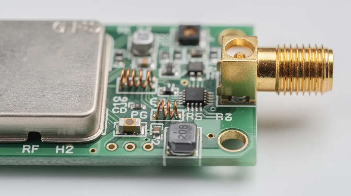
A transmitter sits at the heart of every wireless device you design. It converts data into a radio signal, pushes it through an antenna, and sends it across space. This article covers transmitter design from the PCB engineer’s point of view - substrates, layout, thermal management, shielding, and manufacturability.
Key Takeaways
A transmitter converts data into radio signals or standardized electrical signals. It plays a central role in modern electronic hardware.
RF and wireless transmitters (Wi‑Fi, Bluetooth, LoRa, cellular) demand strict PCB layout control for impedance, grounding, and radio signal integrity.
Power amplifier layout, thermal vias, and copper design define reliability for high‑power radio transmitters on complex boards.
EMI, EMC, and shielding cans protect both the transmitter and nearby circuits from unwanted radio waves and noise.
Robust transmitter performance depends on early collaboration between RF design, PCB layout, and PCB manufacturing teams.
What Is a Transmitter in Modern Electronics?
A transmitter is a circuit or device that converts digital information into a signal that can travel across radio waves, cables, or optical fiber. Transmitters generate signals for wireless data transmission. They also ensure signals remain stable and predictable during transmission.
Three types matter for PCB engineers:
Radio transmitters - RF front ends that produce and transmit electromagnetic waves at a set carrier frequency.
Industrial transmitters - sensor-based devices that amplify and condition sensor signals for transmission over a 4–20 mA loop or digital link. Transmitters can be electronic or pneumatic. Pneumatic transmitters use a 3–15 psig signal range.
Digital wireless modules - pre-certified components that embed radio, power amplifier, and filters on a single board.
Wireless transmitters operate without physical wiring. They are used in harsh industrial environments. They reduce installation costs and maintenance. They also provide quick installation and minimal disruption.
In most PCB designs, the engineer cares about how clean, efficient, and stable that radio signal is. Common carrier frequency ranges in 2024–2026 include:
2.4 GHz and 5 GHz (Wi‑Fi, Bluetooth)
Sub‑GHz ISM: 433 MHz, 868/915 MHz (LoRa, Sigfox)
Cellular bands: 700 MHz up to several GHz (LTE, NB‑IoT, 5G FR1)
Core Elements of a Radio Transmitter Chain
Most radio transmitters on PCBs share a similar block diagram. Data flows from a source through several stages before it reaches the antenna.
Here are the main building blocks:
Baseband or microcontroller - generates the digital information stream.
Modulator - shapes bits into a waveform that rides on a carrier. For example, OFDM for Wi‑Fi or GFSK for Bluetooth.
Frequency synthesizer (PLL + VCO) - locks the carrier to an accurate operating frequency so the radio signal stays inside its channel mask.
Power amplifier (PA) - boosts the electrical signal to the required output power level.
Matching network - converts the PA impedance to the antenna’s 50 Ω using L‑, T‑, or Π‑networks of inductors and capacitors.
Antenna or connector - radiates the radio waves into space or feeds them to a cable.
The matching network between the PA and antenna is one of the most sensitive RF areas. It drives many PCB layout constraints. Even small parasitic inductance from extra trace length can shift impedance and degrade efficiency.
RF & Wireless Transmitter Types on Today’s PCBs
Hardware designers must choose the right radio transmitter for each product. Choosing the right transmitter depends on distance, data needs, and type of signal. Here is a practical overview.
Wi‑Fi transmitters operate at 2.4 GHz and 5 GHz. They appear in routers, IoT gateways, and consumer products. Wi‑Fi is suitable for high-bandwidth needs with permanent AC power availability. Heavy data streams like HD video require alternatives to standard Wi‑Fi, such as COFDM video transmitters that handle multipath interference better.
Bluetooth and Bluetooth Low Energy (BLE) serve short-range links. BLE is ideal for short-range monitoring and smartphone interaction. These transmitters have a small RF footprint on the PCB. Wearables, audio devices, and low-power sensors commonly use them.
LoRa and sub‑GHz ISM transmitters dominate long-range, low-bit-rate communication. LoRa is the industry leader for low-power long-range data transmission. It enables transmission of small data packets over kilometers using minimal power. LoRa offers a range up to 2–15 km in various environments. LoRaWAN is best for long-range low-power deployments. It is optimal for low-power outdoor or industrial sensing applications. LoRa modules are the gold standard for low-power IoT communications. Lower frequencies like 433 MHz and 900 MHz penetrate obstacles better than higher frequencies. Smart meters, agriculture sensors, and warehouse monitoring nodes rely on LoRa.
Cellular transmitters (LTE, LTE‑M, NB‑IoT, 5G FR1) often come as certified modules. They include integrated power amplifiers and RF filters. Cellular technologies are best for standalone remote sensors needing direct cloud connection. Satellite communication systems provide global coverage and work without terrestrial infrastructure.
VHF/UHF transmitters cover ranges from a few miles to tens of miles. HF radio transmitters are best for long distances and can communicate beyond the horizon.
Zigbee is effective for smart home and building automation applications. Mesh networks are ideal for home automation and smart lighting applications.
Choosing a transmitter involves balancing range, power consumption, and data speed. Selecting the right transmitter depends on range, power budget, data volume, and environment. But all these radio transmitters share common layout themes: controlled impedance traces, clean ground planes, tight decoupling, and careful isolation from noisy digital blocks.
PCB Stackup and Substrate Choices for Radio Transmitters
Operating frequency and radio signal bandwidth affect stackup, material, and manufacturing choices. The wrong substrate can eat your entire link budget.
Standard FR‑4 works well for sub‑GHz radio transmitters with short RF paths. But above about 3 GHz, FR‑4’s limits hit hard. Insertion loss rises. Dielectric constant drifts with temperature and frequency.
Here is a comparison based on measured data from Atlas PCB:
| Parameter | FR‑4 | Rogers 4350B |
|---|---|---|
| Insertion loss at 2.4 GHz | ~0.32 dB/in | ~0.14 dB/in |
| Insertion loss at 5.5 GHz | ~0.58 dB/in | ~0.21 dB/in |
| Dk drift (25–85 °C) | ±4–8% | ±1–2% |
| Df (loss tangent) at 10 GHz | ~0.020 | ~0.004 |
| High-frequency laminates like Rogers 4003C or 4350B offer lower loss and stable Dk over temperature. Hybrid stackups combine Rogers on RF layers with FR‑4 for digital and power layers. This approach balances cost vs performance. |
Key material parameters to check in datasheets:
Dielectric constant (Dk)
Dissipation factor (Df or loss tangent)
Thickness tolerance across the RF layer
CTE (especially Z‑axis) and Tg
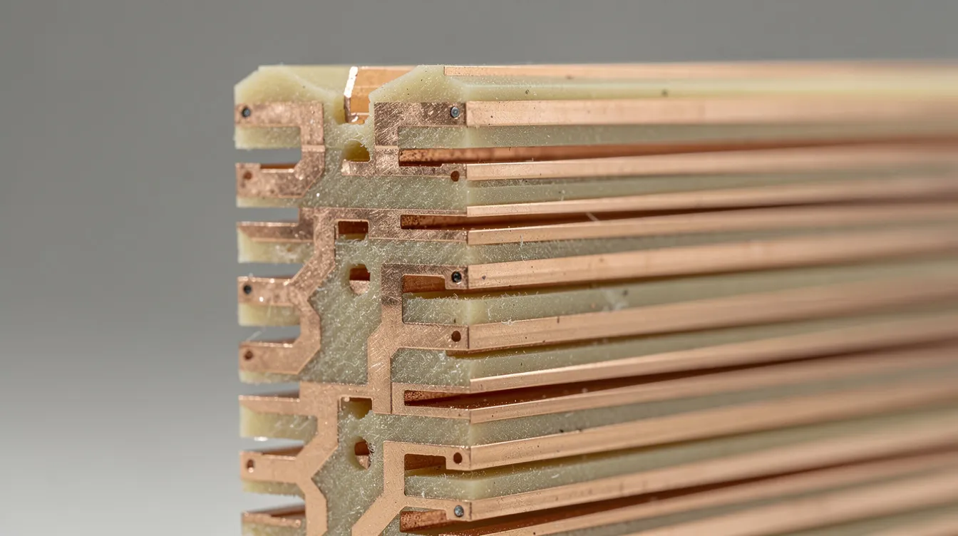
PCB manufacturers build controlled impedance microstrip and stripline traces based on these values. Early DFM checks on the stackup are vital. Substrate choice also affects thermal performance for high-power radio transmitters.
Controlled Impedance, Traces, and Grounding for Radio Signals
Radio transmitter performance ties directly to PCB trace geometry and ground reference quality. A broken return path or wrong trace width can kill your radio signal.
Microstrip vs stripline: Microstrip runs on an outer layer with a ground plane below. Stripline runs between two ground planes on inner layers. Microstrip is easier to probe and tune. Stripline offers better isolation. Grounded coplanar waveguide (GCPW) adds ground rails beside the trace for extra shielding.
Target impedances: Single-ended 50 Ω is standard for PA and antenna ports. Differential traces often target 90–100 Ω. Use field solvers or impedance calculators during design.
Best practices for RF traces:
Keep RF paths short. Every extra millimeter adds loss.
Minimize vias in RF lines. Each via adds parasitic inductance.
Use smooth arcs or mitered bends instead of sharp 90° corners.
Fill or cap vias when they must appear in the RF path.
A continuous ground plane under radio transmitter sections is essential. Use dense stitching vias along RF traces and around the transmitter region. Split grounds (analog, digital, RF) must connect at planned points. Random ground gaps near RF traces deform the radio signal and create unwanted radiation.
Power Amplifier Layout and Thermal Management
Higher-power radio transmitters place power amplifiers close to the antenna feed. PA layout is one of the toughest jobs in RF PCB design.
Placement rules:
Keep the PA close to the antenna or filter output.
Minimize RF trace length between the PA output and matching network.
Orient the PA so its output pins face the matching network pads.
Supply and decoupling:
Use wide copper pours on PA supply lines to reduce voltage droop.
Connect supply pins to internal planes with multiple vias.
Place multi-value decoupling capacitors (10 nF, 1 µF, 10 µF) near each power pin.
Thermal design:
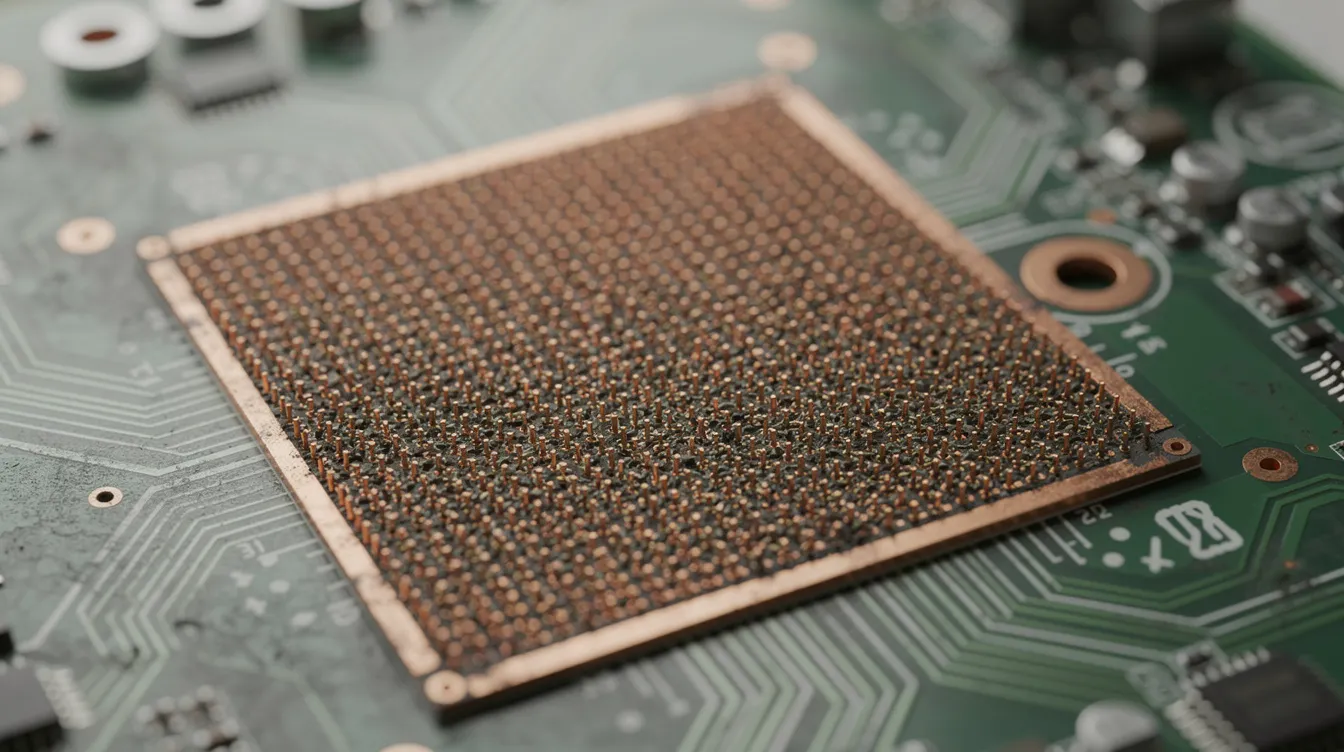
Add a thermal pad under the PA with dense arrays of thermal vias to inner copper or heat spreaders.
Coordinate with metal housings or heat sinks for energy dissipation.
Example: A 2 W LDMOS transmitter stage in the 900 MHz band must keep junction temperature below about 150 °C. This target drives copper thickness (often 2 oz or more), via count (20+ thermal vias under the pad), and board copper plane layout. Without enough thermal vias, the device overheats and output power drops.
Thermal and RF goals can conflict. Extra copper for heat spreading may change the characteristic impedance of nearby traces. Layout engineers must balance copper for thermal management with consistent impedance in RF regions. Antenna elevation can also improve wireless communication range, so PA performance at the board level matters for the whole link.
Decoupling, Power Integrity, and Noise Control in Transmitters
Clean power is critical for stable radio signals, accurate frequency synthesis, and linear PA operation.
Multi-stage decoupling near every RF IC uses a mix of small (10 nF) and larger (1–10 µF) capacitors. Keep traces between capacitors and IC pins short. Long traces add inductance that defeats the capacitor’s purpose.
Power distribution best practices:
Use star routing or dedicated plane splits for analog, RF, and digital supplies.
Prevent large PA current pulses from polluting sensitive PLL or ADC supplies.
Place LC filters or ferrite beads in series with supply rails feeding RF blocks.
Keep switching power stages like DC‑DC converters away from low-level RF inputs and local oscillators. Maintain clear ground separation between them.
Controlled return paths in ground planes prevent hidden loops. These loops radiate and create interference with the radio transmitter. Transmitters amplify and condition sensor signals for transmission, so any noise on the supply chain degrades the received signals at the other end.
EMC, EMI, and Shielding Strategies for Transmitter PCBs
Strong radio transmitters create two risks. First, they can fail EMC tests. Second, they can disturb nearby circuits with unwanted radio waves.
Shielding approaches:
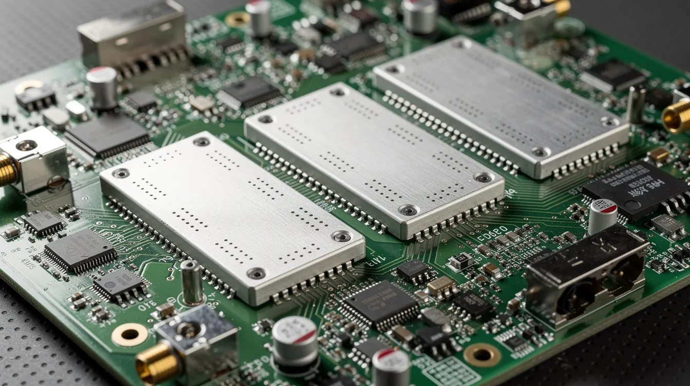
RF cans over the transmitter section block radiated noise.
Via fences beside RF traces form solid ground walls.
Metal enclosures with gasket contact contain the strongest emissions.
Reserve keep-out areas and mechanical anchoring points for shielding cans early in the PCB layout. Don’t treat shielding as an afterthought.
Grounding for shields requires multiple low-inductance connections to the main ground plane. Avoid floating metal islands. These can resonate and make interference worse.
Practical EMC considerations:
Control harmonic content from the radio transmitter with output filters.
High-power transmissions must comply with regulatory limits set by bodies like the FCC.
Run pre-compliance tests before committing to a final design.
Good shielding also protects the receiver and digital logic from the strong local radio signal. This difference matters when transmitter and receiver share the same board, which is common in transceiver equipment.
Industrial and Sensor Transmitters at Hardware Level
Industrial transmitters convert physical variables (pressure, temperature, flow) into standardized electrical signals. The focus here is on the electronic circuit and PCB, not the control room computer.
Typical signal chain:
Sensor element - such as a piezoresistive bridge for a pressure transmitter.
Analog front end - amplifiers, filters, and signal conditioning.
ADC - digitizes the conditioned signal.
Microcontroller - processes data and drives the output.
The microcontroller can produce analog signals like 4–20 mA for communication over a current loop. It can also drive a 0–10 V output. Analog transmitters use a 4–20 mA current signal standard. Digital transmitters enhance communication with various protocols like WirelessHART or proprietary ISM links.
Pressure transmitters measure absolute, gauge, or differential pressure. Level transmitters can be point or continuous measurement types. Transmitters convert signals into standardized formats for transmission. Wireless transmitters translate data into comprehensible forms.
Example: A pressure transmitter samples a piezoresistive bridge sensor. The analog front end amplifies the weak bridge output. The ADC digitizes it. The microcontroller then sends data via a sub-GHz radio transmitter to a gateway several kilometers away. This form of remote monitoring is common in oil and gas industries.
Industrial transmitters often sit in harsh environments. Designers must consider conformal coating, isolation gaps, surge protection (TVS diodes), and robust connectors. Even when no RF section exists, careful grounding and filtering protect these transmitters from industrial EMI and transient events.
Transmitter PCB Design for Manufacturability (DFM)
Transmitter performance ties to realistic PCB manufacturing and SMT assembly limits. Tolerances on trace width and dielectric thickness affect your RF results.
Coordinate early with the fabricator to lock:
Stackup and material callouts
Copper weight (1 oz, 2 oz, or heavier)
Controlled impedance tolerances (e.g., 50 Ω ±5%)
Minimum via dimensions for RF sections
RF pads, matching networks, and small components around the radio transmitter must follow assembly rules. Solder fillets, stencil apertures, and inspection access all need attention.
Shield cans, large RF connectors, and heat sinks require mechanical keepouts. Plan panelization so contract manufacturers can assemble and reflow boards with low risk.
Include test points or RF connectors for radio signal validation and calibration. Place them where they won’t disturb the RF path.
Tight collaboration between RF engineers, PCB layout staff, and the manufacturing partner shortens debug cycles and improves first-pass yield.
Engineering Comparison Table: Transmitter Types vs Layout Needs
This table helps engineers compare radio transmitters and industrial transmitters from a PCB design point of view.
| Transmitter Type | Typical Frequency | Main Use Cases | PCB Layout Challenges | Recommended Substrate | Example Standard |
|---|---|---|---|---|---|
| Wi‑Fi | 2.4 GHz, 5 GHz | Routers, IoT gateways, consumer devices | High-frequency impedance control, EMC compliance, dense digital nearby | FR‑4 (2.4 GHz short runs), Rogers hybrid (5 GHz) | IEEE 802.11ax |
| Bluetooth / BLE | 2.4 GHz | Wearables, audio, sensors | Small footprint, antenna placement, low power | FR‑4 with controlled impedance | Bluetooth 5.x |
| LoRa / Sub‑GHz ISM | 433 MHz, 868/915 MHz | Smart meters, agriculture, warehouse sensors | Antenna matching at lower frequencies, long traces acceptable on FR‑4 | Standard FR‑4 | LoRaWAN |
| Cellular (LTE/NB‑IoT/5G) | 700 MHz – 6 GHz | Remote monitoring, fleet tracking, location services | Module placement, multi-band antenna, thermal for PA | FR‑4 or hybrid per module datasheet | 3GPP LTE Cat‑M1 |
| Industrial 4–20 mA | DC (baseband) | Pressure, temperature, flow sensing | Analog noise isolation, current loop routing, surge protection | Standard FR‑4 | HART, 4–20 mA |
| Choosing the best long-distance wireless transmitter depends on use case. LoRa transmitters can transmit several miles or more depending on conditions. Cellular modules give you direct cloud connection. VHF/UHF radios cover tens of miles for voice or data. |
Conclusion: Building Robust Transmitter PCBs
Clean radio signals start with sound PCB engineering. Stackup choice, controlled impedance routing, PA thermal management, and shielding define whether a radio transmitter meets performance and regulatory targets.
Incorporate DFM principles during schematic and layout. The final PCB must align with what modern manufacturing and SMT assembly lines can deliver. A person designing a transmitter board should treat the fabricator as a core team member, not an afterthought.
Involve your PCB manufacturing partner early when planning new RF or industrial transmitter designs. Early DFM reviews save time, money, and redesign cycles.
FAQ
These FAQs cover practical transmitter design questions not addressed in the main sections.
How close can I place digital circuits near a radio transmitter section?
Keep fast digital buses and clock lines several millimeters from RF traces. Place a solid ground barrier between the two regions. Route high-speed digital lines on different layers. A continuous ground plane between those layers and the RF layer cuts crosstalk into the radio signal.
Critical areas like the PA output and matching network need clear space. Avoid noisy traces on all layers under and adjacent to these RF components.
When do I need a dedicated RF ground plane?
Small, low-power transmitters at 2.4 GHz often work fine with a shared ground plane. The RF area must remain clean and continuous.
Higher-power transmitters or crowded mixed-signal boards may benefit from a locally dedicated RF ground region. Tie it to the main ground at one or a few controlled points. The decision depends on frequency, power level, board size, and how much noise the digital sections produce.
Can I use standard FR‑4 for a 5 GHz radio transmitter?
Many consumer designs use FR‑4 at 5 GHz. But losses and impedance variation increase. Layout margins shrink.
For short RF traces and integrated antennas on small boards, FR‑4 can work if the stackup is tightly controlled. For long RF runs, high output power, or strict link budgets, consider higher-performance laminates or hybrid stackups.
How do I prototype and tune the matching network for my transmitter?
Start from the reference design in the RF IC datasheet. Then adjust component values using a vector network analyzer. Place extra component pads in the matching area during layout. This lets the lab team swap values without redesigning the board.
Small changes in trace length, grounding, or enclosure geometry can shift impedance. Final tuning should occur on hardware that matches the production layout.
What PCB documentation helps a fabricator build RF boards correctly?
Key items include:
Locked stackup with material names and Dk values
Controlled impedance notes with target values and tolerances
Layer diagrams showing RF trace locations
Special finish requirements (ENIG or ENEPIG) on antenna areas
Keepout drawings for shields and antennas
Test coupon requirements so the manufacturer can verify RF trace impedance
Share this documentation early. It prevents costly misunderstandings during fabrication and helps the fabricator listen to your design intent.